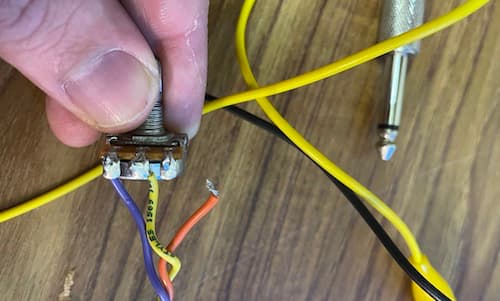
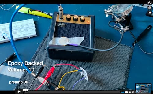
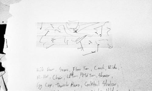
I’m late to this game and missed the connection to the Baltimore late-90s noise scene. I spotted some odd wooden devices in the shop window of Patch Point a couple of years ago. Peter Blasser’s world of weird audio electronics has been seeping in ever since.
Of particular note are his ‘Paper Circuits’. Nothing fancy, no conductive ink, just a print at home substrate for poking and soldering components. They’re a low-cost, accessible entry point for making. Well sort of. They come with a level of esoteric symbolism to decipher. Still, it’s easy to get the hang of, and there’s enough online documentation.
I’ve been making the Lil’ Sidrassi; a noisily-wild touch interfaced synth. I’ve gone through several iterations; there’s some out in the wild amongst friends; I’ll share much more of this in the future. Unfortunately, Covid-19 lockdown has prevented me from launching a series of workshops. I’ll reassess when sensible/safe though.
Working on paper has given me a whole new relationship to building, tinkering, prototyping, and relating to my materials. Twisting, knotting, and threading component legs and wires feels closer to textiles. As great as this is, it’s also time-consuming. Building on paper takes longer than building on a Printed Circuit Board (PCB). There’s also more chance of crossed wires and less chance of durability. Transferring these paper circuits to PCB has benefits, especially if hoping to build at scale.
The final bit of pre-amble I wish to mention is working with PCB software. Briefly, my experiences have been less than positive. I’ve faced either a lack of features or bloated over-complexity for my needs—–the idea of ‘drawing’ my circuits appeals far more. Parts libraries are a bore and drawing my own, developing a more personal language, also appeals. Blasser’s paper circuits were all designed using (Mac only) Osmond PCB. I struggled to understand it at first. Taking Blasser’s freely published source files, I hoped to reverse engineer this process and learn how to do it myself.
I Don’t Have Time For All Of This
No worries, I’m sharing all of this work on GitLab - https://gitlab.com/tripping-on-wires/ciat-lonbarde-pcbs
Credit Where It’s Due
I go into more detail within the GitLab repo but thanks to: Peter Blasser/Ciat Lonbarde for publishing the source files; mlogger/mudlogger, Jason Taylor, and Phil Julian for instructions and advice; and the developers of Osmond PCB for their free software (donate if you can).
Tutorial
We’re going to use Osmond (make sure this is installed) to open Blasser’s paper circuit files and then we’re going to make some minor alterations to get them ready for PCB manufacture. I’m no expert, but this represents some basic functional knowledge I have picked up and which works for me.
Renaming and Opening the Files
First off, the files don’t have the needed .osm extension.
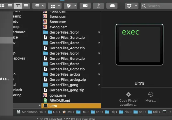
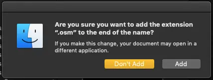
Rename, in finder, adding .osm at the end.

When prompted, click ‘add’, to add the extension.
If successful, the icon and preview will likely change.
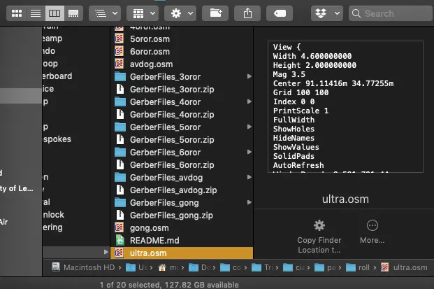
Double click this, and it should open in Osmond (you did install that already didn’t you?).
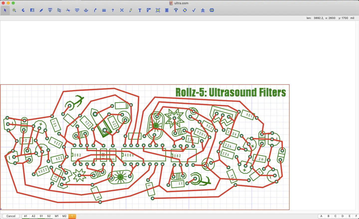
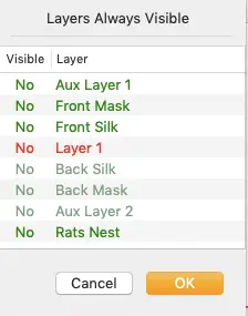
It’s not essential, but I find it easier to set visibility of all layers to ‘No’. This way, you only see the active layer, and you can run through them to check things as you go.
Under the ‘View’ menu select ‘Layers Visible…’
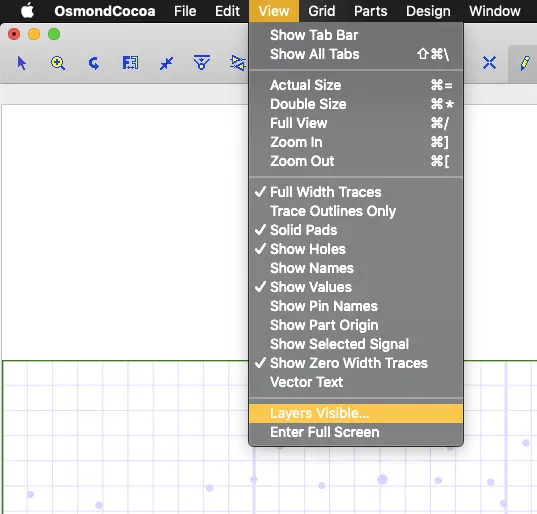
In the popup menu, click all the layers to ‘No’ under ‘Visible’.
A note on Layers. In the bottom left corner, you can select the various layers. Here we have Auxiliary 1 and 2, Screen 1 and 2, Mask 1 and 2, and Layer 1. They all perform slightly different functions, some of which will be covered later.

Moving Traces to the Bottom Layer
For now, we need to make sure we’ve selected Layer 1 (it should be highlighted if it’s selected).
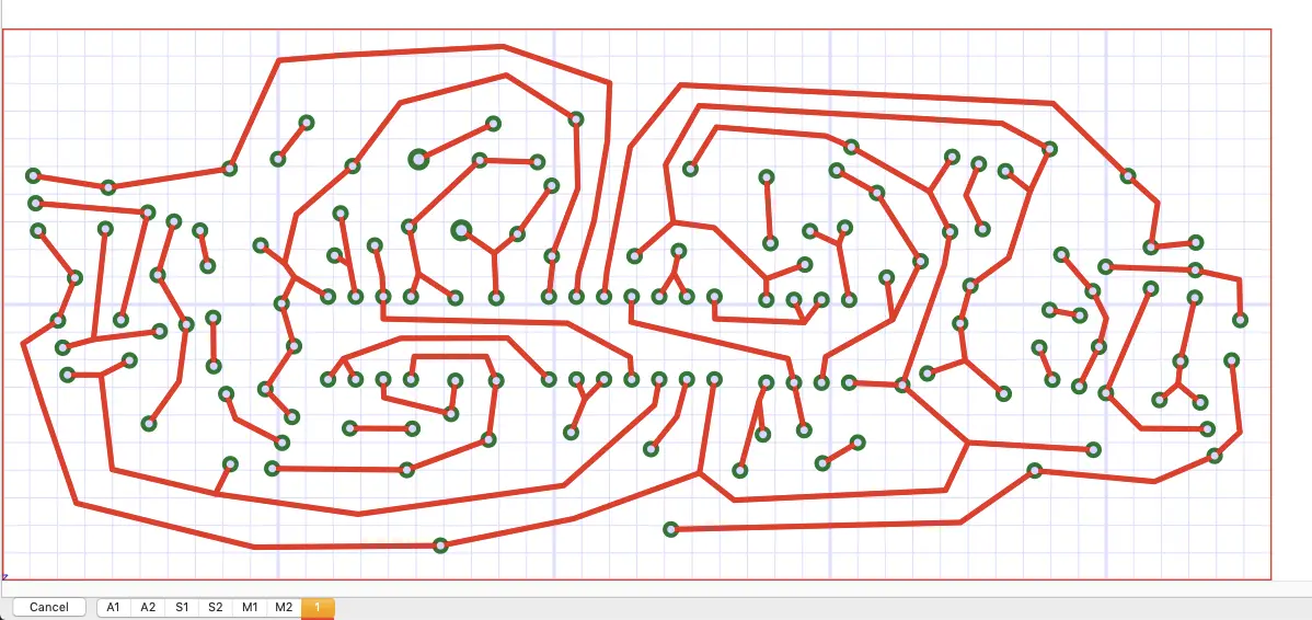
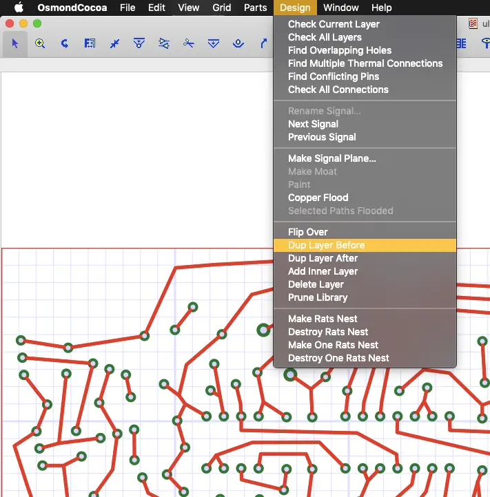
This layer has all the connecting lines on it. These are the connecting traces. While it is possible to have dual-layered (or more) boards, with traces on the top and bottom, I want to keep it simple. At the moment, the solder traces, as the only layer, are on the top. We can add another layer to move things around. Select ‘Design > Dup Layer Before’.
This copies the ‘pads’ (the little solder rings around the holes) but not the ‘paths’ (the traces between components).
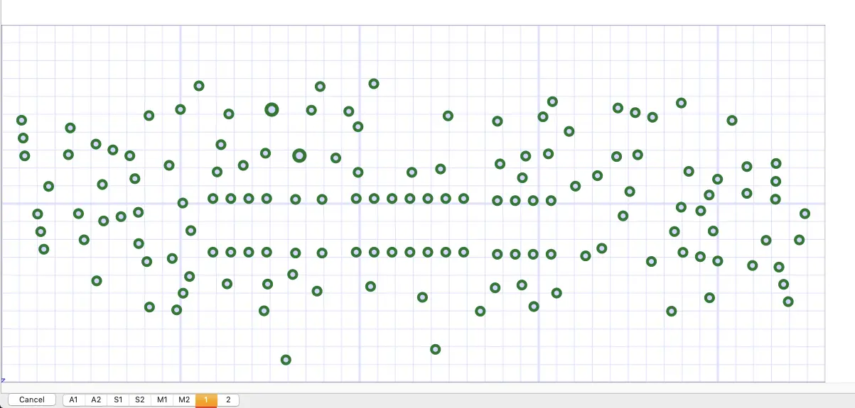
It means we have a ‘blank’ (except for the pads) top layer and all the connections on the bottom layer. We’ve essentially moved things down a layer.
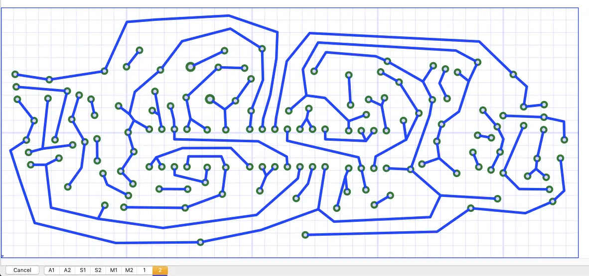
Duplicating the Solder Mask
Next, the solder mask, the coloured lacquer that coats the PCB needs sorting out. Layers M1 and M2 have rings marked that go around component holes. The ‘mask’ is applied around these. If it goes over them, you won’t be able to solder onto it. Currently, M1 has the holes masked properly (the traces were originally on the top layer).

M2 only shows the actual drill holes but not the solder mask rings. If this went to production, the solder pads would be covered over, and we’d have nothing to solder to.
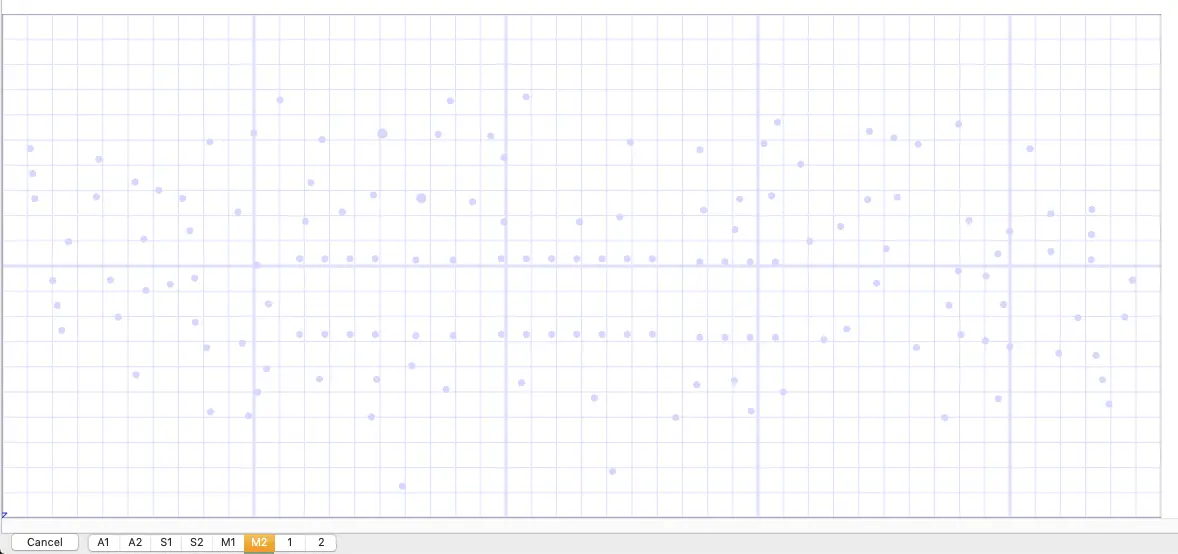
To correct this, we’re going to copy everything on M1 and paste it into M2.
Select layer M1. Cmd+A (or Edit > Select All) followed by Cmd+C (or Edit > Copy). Next select layer M2. Don’t click anywhere or it’ll set the origin point for pasting, and things may be out of alignment. Cmd+V (or Edit > Paste).
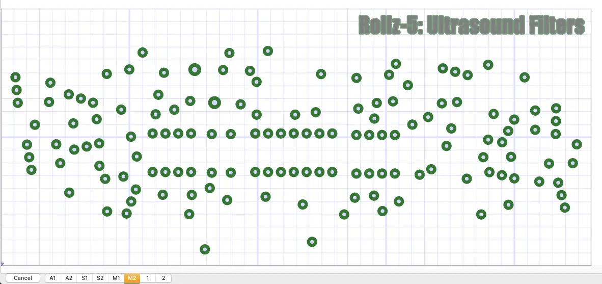
It may have pasted some text too (on the Rollz it pastes the name of the board) if so, click on the text and delete (backspace).
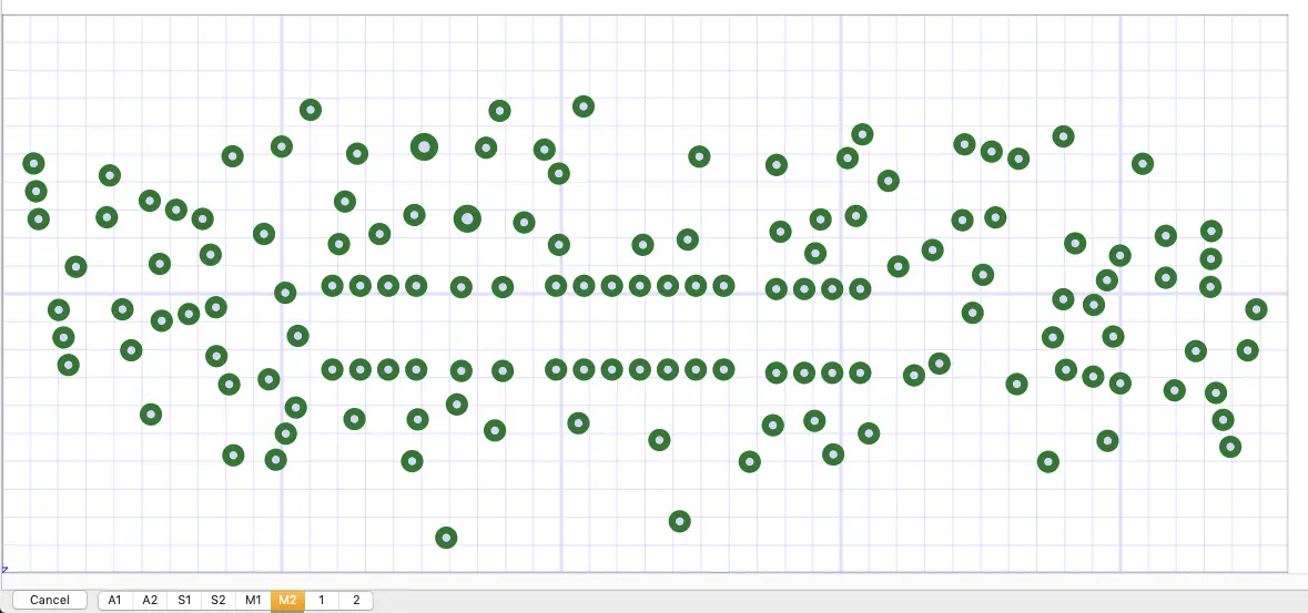
Adding the Board Edge
The next stage is to add the board edge. I had errors when submitting files for production until I corrected this. Previously, I used a convoluted process between Osmond and KiCad, but this is much simpler.
Go to Layer A1.
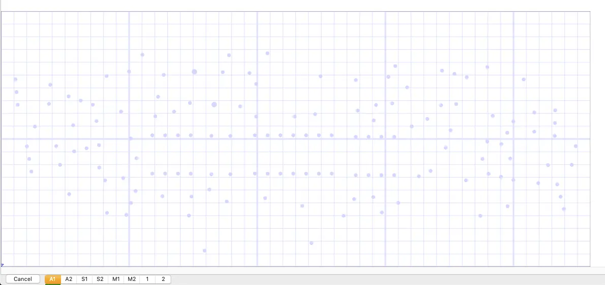
Select the pen tool.

Draw a box around the edge of the design (it’s hard to see in the screenshot but the green box right up to the edges).
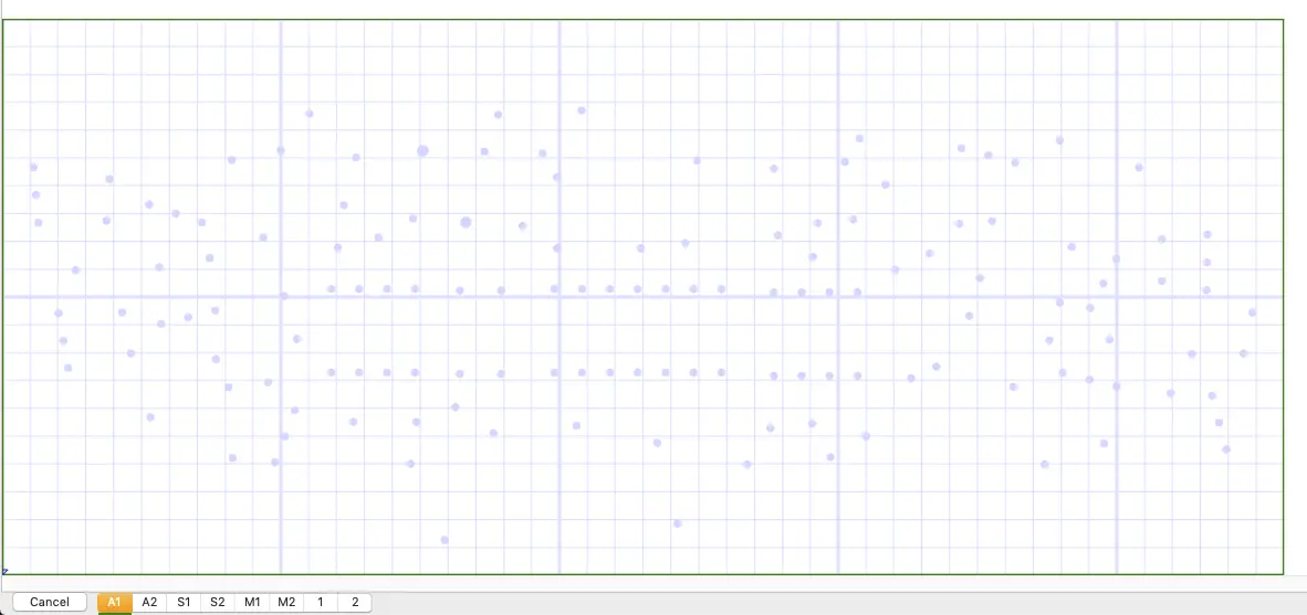
Exporting to Gerber
I now like to make all the layers visible again (View > Layers Visible…) for final checks.
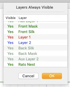
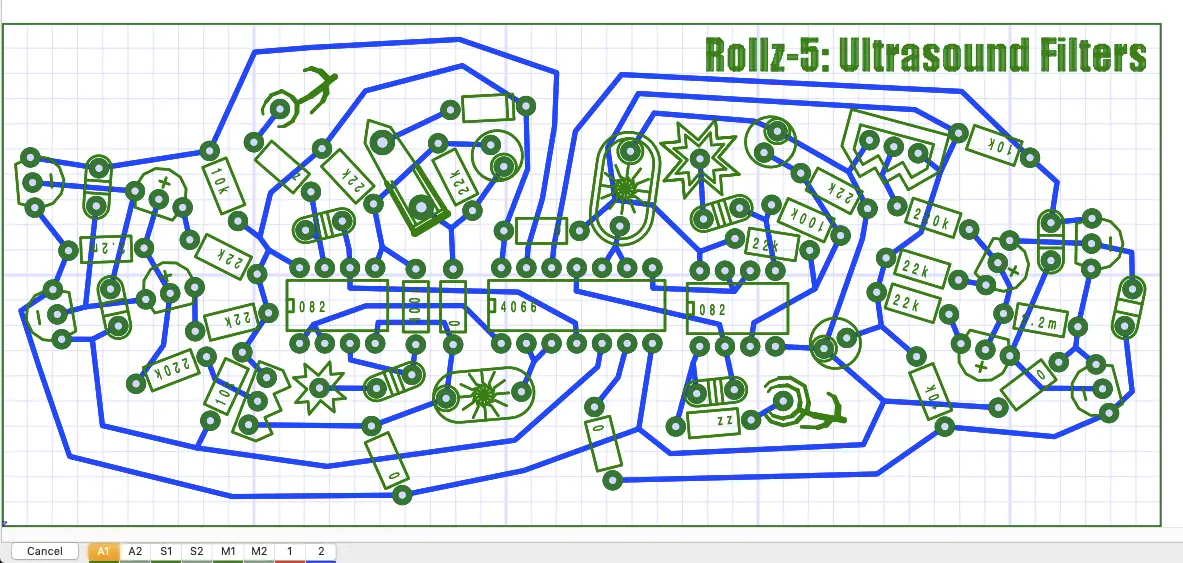
Providing everything looks good we need to get things ready for export. We’re going to generate Gerber files which can be submitted to PCB manufacturers. My experience was that certain file-naming conventions are required. We can use Osmond’s settings to determine this before export (rather than renaming all the files after export).
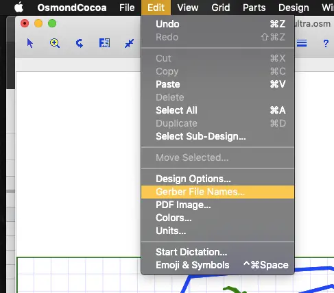
Go to Edit > Gerber File Names…
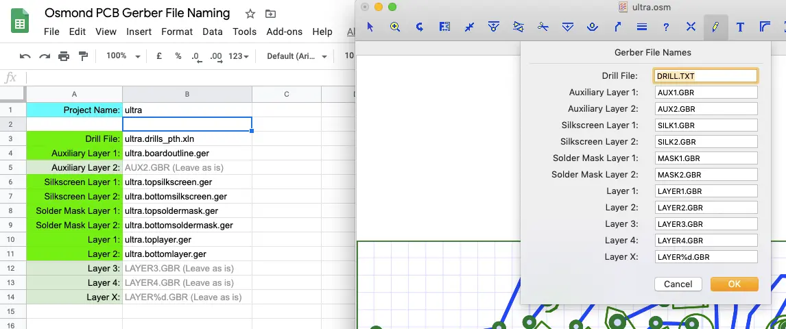
Use the following naming convention (where foo is the project name, i.e. ultra):
- Drill File: foo.drills_pth.xln
- Auxiliary Layer 1: foo.boardoutline.ger
- Auxiliary Layer 2: AUX2.GBR (Leave as is)
- Silkscreen Layer 1: foo.topsilkscreen.ger
- Silkscreen Layer 2: foo.bottomsilkscreen.ger
- Solder Mask Layer 1: foo.topsoldermask.ger
- Solder Mask Layer 2: foo.bottomsoldermask.ger
- Layer 1: foo.toplayer.ger
- Layer 2: foo.bottomlayer.ger
- Layer 3: LAYER3.GBR (Leave as is)
- Layer 4: LAYER4.GBR (Leave as is)
- Layer X: LAYER%d.GBR (Leave as is)
There’s a handy gSheet for calculating these here - https://docs.google.com/spreadsheets/d/1oP2Sg7Z93opfU3iwMOnj0NdZfqy-qCHH4izzCqyGZlc/edit?usp=sharing
I took the screenshot before rather than after but just copy/paste the text into Osmond, one line at a time.
That’s everything all set up. We can now export.
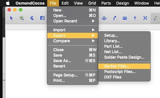
File > Export > Gerber Files… and leave the standard selections.
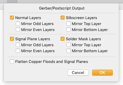
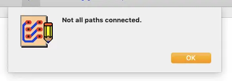
Sometimes, but not always, I get a warning about all paths not being connected. Others, on forums, report that this can be ignored. So far so good for me too, but I’ll report back if there are are any updates here.
You should end up with a folder full of files.
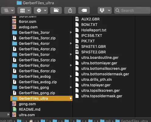
I prefer to create a zip file of these. I find it easier to upload the one zip file to manufacturers rather than a folder of files. I’ll presume you know how to do this and won’t repeat the steps here.
Final Notes
I’ve been using JLCPCB for manufacturing, and the above method has worked for me. I’d recommend making use of any Gerber checking function your manufacturer has available.
If the steps have worked for you, you will have added the .osm extension and opened the files in Osmond. You will have moved the traces to the bottom layer and added the solder mask to this layer. Finally, you will have added the board edge and exported correctly named Gerber files.
Feel free to do this yourself, or use the ones I prepared earlier - https://gitlab.com/tripping-on-wires/ciat-lonbarde-pcb

